1. Product Characteristics and Structural Integrity
1.1 Innate Characteristics of Silicon Carbide
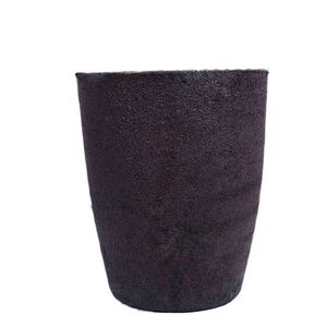
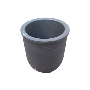
(Silicon Carbide Crucibles)
Silicon carbide (SiC) is a covalent ceramic substance composed of silicon and carbon atoms set up in a tetrahedral latticework framework, largely existing in over 250 polytypic forms, with 6H, 4H, and 3C being the most technically appropriate.
Its solid directional bonding conveys exceptional hardness (Mohs ~ 9.5), high thermal conductivity (80– 120 W/(m · K )for pure solitary crystals), and impressive chemical inertness, making it one of the most durable materials for severe environments.
The broad bandgap (2.9– 3.3 eV) makes certain outstanding electric insulation at area temperature level and high resistance to radiation damage, while its reduced thermal growth coefficient (~ 4.0 × 10 ⁻⁶/ K) contributes to exceptional thermal shock resistance.
These intrinsic properties are protected even at temperatures exceeding 1600 ° C, permitting SiC to maintain structural integrity under prolonged exposure to thaw metals, slags, and reactive gases.
Unlike oxide porcelains such as alumina, SiC does not react conveniently with carbon or type low-melting eutectics in reducing environments, an essential benefit in metallurgical and semiconductor processing.
When made right into crucibles– vessels designed to have and heat products– SiC outshines standard materials like quartz, graphite, and alumina in both life-span and procedure integrity.
1.2 Microstructure and Mechanical Stability
The performance of SiC crucibles is carefully tied to their microstructure, which relies on the manufacturing technique and sintering additives used.
Refractory-grade crucibles are generally generated through reaction bonding, where permeable carbon preforms are infiltrated with liquified silicon, forming β-SiC via the response Si(l) + C(s) → SiC(s).
This procedure generates a composite framework of main SiC with residual cost-free silicon (5– 10%), which boosts thermal conductivity but might limit usage above 1414 ° C(the melting factor of silicon).
Alternatively, completely sintered SiC crucibles are made through solid-state or liquid-phase sintering utilizing boron and carbon or alumina-yttria additives, accomplishing near-theoretical thickness and higher pureness.
These show premium creep resistance and oxidation stability yet are extra costly and challenging to make in large sizes.
( Silicon Carbide Crucibles)
The fine-grained, interlocking microstructure of sintered SiC provides exceptional resistance to thermal exhaustion and mechanical disintegration, vital when dealing with molten silicon, germanium, or III-V compounds in crystal development processes.
Grain border design, consisting of the control of additional stages and porosity, plays an essential function in establishing long-lasting toughness under cyclic heating and hostile chemical environments.
2. Thermal Efficiency and Environmental Resistance
2.1 Thermal Conductivity and Warm Circulation
Among the defining benefits of SiC crucibles is their high thermal conductivity, which enables quick and consistent heat transfer throughout high-temperature processing.
As opposed to low-conductivity products like integrated silica (1– 2 W/(m · K)), SiC efficiently distributes thermal power throughout the crucible wall, lessening localized locations and thermal gradients.
This uniformity is necessary in processes such as directional solidification of multicrystalline silicon for photovoltaics, where temperature homogeneity directly influences crystal quality and problem density.
The combination of high conductivity and low thermal growth causes an incredibly high thermal shock parameter (R = k(1 − ν)α/ σ), making SiC crucibles immune to splitting during quick heating or cooling down cycles.
This allows for faster heater ramp rates, enhanced throughput, and decreased downtime as a result of crucible failing.
Furthermore, the material’s capability to hold up against duplicated thermal cycling without significant deterioration makes it excellent for set processing in industrial furnaces operating above 1500 ° C.
2.2 Oxidation and Chemical Compatibility
At elevated temperatures in air, SiC goes through easy oxidation, forming a safety layer of amorphous silica (SiO TWO) on its surface area: SiC + 3/2 O TWO → SiO TWO + CO.
This glazed layer densifies at heats, serving as a diffusion obstacle that slows down additional oxidation and maintains the underlying ceramic structure.
Nevertheless, in decreasing ambiences or vacuum cleaner problems– typical in semiconductor and metal refining– oxidation is suppressed, and SiC continues to be chemically steady against molten silicon, aluminum, and many slags.
It stands up to dissolution and response with liquified silicon up to 1410 ° C, although long term exposure can lead to small carbon pickup or user interface roughening.
Most importantly, SiC does not introduce metallic pollutants right into sensitive melts, a crucial demand for electronic-grade silicon production where contamination by Fe, Cu, or Cr must be kept below ppb degrees.
Nonetheless, care has to be taken when processing alkaline planet metals or extremely responsive oxides, as some can corrode SiC at extreme temperature levels.
3. Production Processes and Quality Assurance
3.1 Manufacture Methods and Dimensional Control
The production of SiC crucibles entails shaping, drying out, and high-temperature sintering or seepage, with approaches picked based upon called for purity, dimension, and application.
Typical creating techniques consist of isostatic pressing, extrusion, and slip spreading, each using different degrees of dimensional accuracy and microstructural uniformity.
For large crucibles utilized in photovoltaic ingot spreading, isostatic pressing ensures constant wall density and thickness, decreasing the danger of crooked thermal development and failure.
Reaction-bonded SiC (RBSC) crucibles are economical and extensively made use of in foundries and solar sectors, though residual silicon limitations maximum solution temperature level.
Sintered SiC (SSiC) versions, while more expensive, offer remarkable pureness, strength, and resistance to chemical strike, making them suitable for high-value applications like GaAs or InP crystal growth.
Accuracy machining after sintering may be called for to achieve tight tolerances, specifically for crucibles utilized in vertical gradient freeze (VGF) or Czochralski (CZ) systems.
Surface area ending up is crucial to reduce nucleation sites for flaws and make sure smooth melt flow throughout spreading.
3.2 Quality Assurance and Performance Recognition
Rigorous quality assurance is important to ensure dependability and long life of SiC crucibles under requiring functional problems.
Non-destructive evaluation techniques such as ultrasonic testing and X-ray tomography are used to spot interior cracks, gaps, or thickness variants.
Chemical evaluation by means of XRF or ICP-MS verifies reduced degrees of metal pollutants, while thermal conductivity and flexural stamina are gauged to validate material consistency.
Crucibles are frequently based on substitute thermal biking examinations before shipment to identify possible failure settings.
Batch traceability and accreditation are common in semiconductor and aerospace supply chains, where part failure can bring about pricey production losses.
4. Applications and Technical Impact
4.1 Semiconductor and Photovoltaic Industries
Silicon carbide crucibles play a critical function in the production of high-purity silicon for both microelectronics and solar batteries.
In directional solidification furnaces for multicrystalline photovoltaic or pv ingots, big SiC crucibles serve as the key container for molten silicon, enduring temperatures over 1500 ° C for several cycles.
Their chemical inertness prevents contamination, while their thermal security ensures consistent solidification fronts, causing higher-quality wafers with less misplacements and grain borders.
Some producers coat the internal surface with silicon nitride or silica to even more reduce bond and facilitate ingot release after cooling down.
In research-scale Czochralski growth of substance semiconductors, smaller SiC crucibles are used to hold melts of GaAs, InSb, or CdTe, where marginal sensitivity and dimensional stability are extremely important.
4.2 Metallurgy, Foundry, and Arising Technologies
Beyond semiconductors, SiC crucibles are indispensable in steel refining, alloy preparation, and laboratory-scale melting procedures including light weight aluminum, copper, and precious metals.
Their resistance to thermal shock and disintegration makes them perfect for induction and resistance heaters in factories, where they outlive graphite and alumina choices by a number of cycles.
In additive production of reactive steels, SiC containers are made use of in vacuum induction melting to prevent crucible malfunction and contamination.
Arising applications consist of molten salt activators and concentrated solar power systems, where SiC vessels might include high-temperature salts or fluid steels for thermal power storage.
With recurring developments in sintering innovation and finishing design, SiC crucibles are poised to support next-generation products handling, making it possible for cleaner, extra reliable, and scalable commercial thermal systems.
In summary, silicon carbide crucibles stand for a vital allowing innovation in high-temperature product synthesis, integrating outstanding thermal, mechanical, and chemical performance in a single engineered element.
Their prevalent fostering across semiconductor, solar, and metallurgical sectors emphasizes their function as a cornerstone of modern-day industrial ceramics.
5. Vendor
Advanced Ceramics founded on October 17, 2012, is a high-tech enterprise committed to the research and development, production, processing, sales and technical services of ceramic relative materials and products. Our products includes but not limited to Boron Carbide Ceramic Products, Boron Nitride Ceramic Products, Silicon Carbide Ceramic Products, Silicon Nitride Ceramic Products, Zirconium Dioxide Ceramic Products, etc. If you are interested, please feel free to contact us.
Tags: Silicon Carbide Crucibles, Silicon Carbide Ceramic, Silicon Carbide Ceramic Crucibles
All articles and pictures are from the Internet. If there are any copyright issues, please contact us in time to delete.
Inquiry us